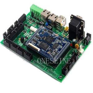
Cheapest High Frequency Prototype Quick Turn Pcb Pcba Assembly
Basic information:
Layer:2
Material:Rogers
PCB thickness:1.6mm
Copper weight:35um
Surface finish: HASL lead free
Service:PCB and components sourcing and assembly
Required files:gerber and bom list
Quantity:10 sets
Prototype PCB Assembly service:
Surface Mount PCB assembly (Both rigid PCB, flexible PCB)
PCBA contract manufacturing;
Electronic contract manufacturing service
Through hole assembly/DIP assembly;
Bonding assembly;
Final assembly;
Full Turnkey Box Build;
Mechanical / electrical assembly
Supply Chain Management/Components procurement;
PCB fabrication;
Technical support / OEM/ ODM service
NO MOQ, from Prototype, Small Volume to Middle Volume production.
We can accept CAM350, GC-CAM, GERBER PROTEL 99SE, CAM Drawing for producing PCBs;
We have end-to-end WIP online order tracking system to manager each process of your products and ensure our quality for timely delivery;
ONESEINE follow Strict QC Spec to deliver good and safe boards to our customers'hand Once the mass production starts, we will monitor the output status on regular basis through the daily WIP status reports and ERP data to ensure on-time delivery.
Prototype PCB Assembly delivery time:
Components sourcing:5-12 days according to the components model
PCB:3-5 days
Assembly:3 days
The PCB assembly process typically includes the following steps:
Component Procurement: The required electronic components are sourced from suppliers. This involves selecting components based on specifications, availability, and cost.
PCB Fabrication: The bare PCBs are manufactured using specialized techniques such as etching or printing. The PCBs are designed with copper traces and pads to establish electrical connections between the components.
Component Placement: Automated machines, called pick-and-place machines, are used to accurately place surface mount components (SMD components) on the PCB. These machines can handle a large number of components with precision and speed.
Soldering: Once the components are placed on the PCB, soldering is performed to establish electrical and mechanical connections. There are two common methods used for soldering: a. Reflow Soldering: This method involves applying solder paste to the PCB, which contains small solder balls. The PCB is then heated in a reflow oven, causing the solder to melt and create connections between the components and the PCB. b. Wave Soldering: This method is typically used for through-hole components. The PCB is passed over a wave of molten solder, which creates solder connections on the bottom side of the board.
Inspection and Testing: After soldering, the assembled PCBs undergo inspection to check for defects, such as solder bridges or missing components. Automated optical inspection (AOI) machines or human inspectors perform this step. Functional testing may also be conducted to ensure the PCB operates as intended.
Final Assembly: Once the PCBs pass inspection and testing, they can be integrated into the final product. This may involve additional assembly steps, such as attaching connectors, cables, enclosures, or other mechanical components.